- 您现在的位置:买卖IC网 > Sheet目录2006 > LTC2755AIUP-16#PBF (Linear Technology)IC DAC 16BIT CUR OUT 64-QFN
LTC2755
20
2755f
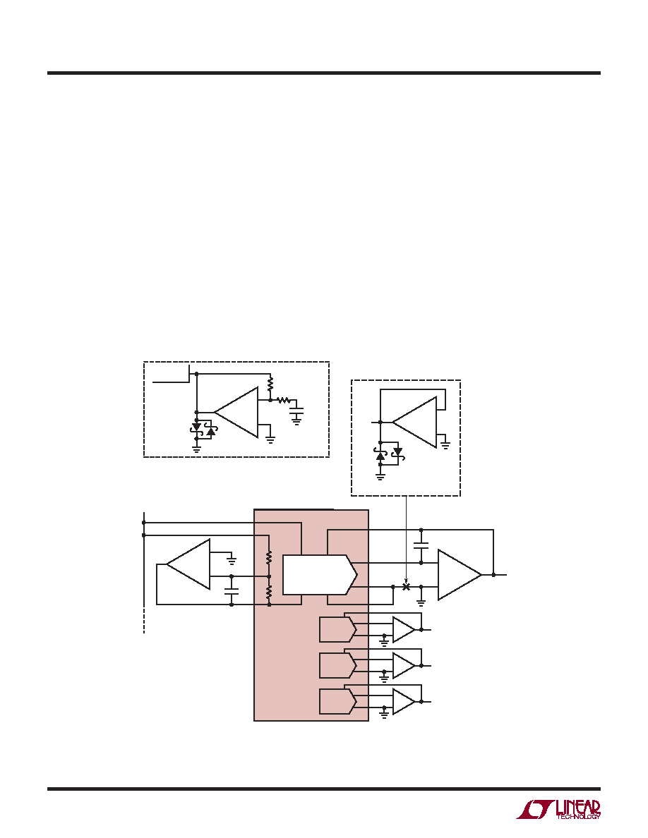
Grounding
As with any high resolution converter, clean grounding is
important. A low impedance analog ground plane and star
grounding techniques should be used. IOUT2X must be tied
to the star ground with as low a resistance as possible.
When it is not possible to locate star ground close to
IOUT2, a low resistance trace should be used to route this
pin to star ground. This minimizes the voltage drop from
this pin to ground caused by the code dependent current
owing to ground. When the resistance of this circuit
board trace becomes greater than 1Ω, a force/sense am-
plier conguration should be used to drive this pin (see
APPLICATIONS INFORMATION
Figure 2). This preserves the excellent accuracy (1LSB
INL and DNL) of the LTC2755-16.
Layout
Figures 3, 4, 5, and 6 show the layout for the LTC2755
evaluation board, DC1112. This shows how to route
the digital signals around the device without interfering
with the reference and output op amps. Complete demo
board documentation is available in the DC1112 quick
start guide.
–
+
–
+
1/2 LT1469
DAC A
LTC2755-16
VREF
5V
2
1
3
59
60
61
64
63
1
62
IOUT1A
15pF
IOUT2A
RFBA
RVOSA
REFA
RCOM1
RIN1
ROFSA
VOUTA
2
58
–
+
6
1
23
IOUT2
2
3
*SCHOTTKY BARRIER DIODE
ZETEX*
BAT54S
LT1001
2755 F02
1000pF
ALTERNATE AMPLIFIER FOR OPTIMUM SETTLING TIME PERFORMANCE
6
1
23
2,14, 34, 46
–
+
LT1468
3
ZETEX
BAT54S
2
200Ω
IOUT2
150pF
3
2
DAC B
DAC C
DAC D
–
+
–
+
–
+
Figure 2. Optional Circuits for Driving IOUT2 from GND with a Force/Sense Amplier.
发布紧急采购,3分钟左右您将得到回复。
相关PDF资料
LTC2757ACLX#PBF
IC DAC 18BIT PAR 48LQFP
LTC2758AILX#PBF
IC DAC 18BIT SPI/SRL 48-LQFP
LTC2844IG#TRPBF
IC TXRX 3.3V MULTIPROTCOL 28SSOP
LTC2852MPS#PBF
IC TXRX RS485 20MBPS 14-SOIC
LTC486ISW#TRPBF
IC DVR RS485 LOW PWR QUAD 16SOIC
LTC490IS8#TRPBF
IC TXRX RS485 LOW POWER 8-SOIC
LTC491IS#TRPBF
IC TXRX RS485 LOW POWER 14-SOIC
LTC6900IS5#TR
IC OSC SILICON 20MHZ TSOT23-5
相关代理商/技术参数
LTC2755AIUP-16#TRPBF
功能描述:IC DAC 16BIT CUR OUT 64-QFN RoHS:是 类别:集成电路 (IC) >> 数据采集 - 数模转换器 系列:SoftSpan™ 产品培训模块:Data Converter Fundamentals
DAC Architectures 标准包装:750 系列:- 设置时间:7µs 位数:16 数据接口:并联 转换器数目:1 电压电源:双 ± 功率耗散(最大):100mW 工作温度:0°C ~ 70°C 安装类型:表面贴装 封装/外壳:28-LCC(J 形引线) 供应商设备封装:28-PLCC(11.51x11.51) 包装:带卷 (TR) 输出数目和类型:1 电压,单极;1 电压,双极 采样率(每秒):143k
LTC2755BCUP-16#PBF
功能描述:IC DAC 16BIT CUR OUT 64-QFN RoHS:是 类别:集成电路 (IC) >> 数据采集 - 数模转换器 系列:SoftSpan™ 标准包装:1 系列:- 设置时间:4.5µs 位数:12 数据接口:串行,SPI? 转换器数目:1 电压电源:单电源 功率耗散(最大):- 工作温度:-40°C ~ 125°C 安装类型:表面贴装 封装/外壳:8-SOIC(0.154",3.90mm 宽) 供应商设备封装:8-SOICN 包装:剪切带 (CT) 输出数目和类型:1 电压,单极;1 电压,双极 采样率(每秒):* 其它名称:MCP4921T-E/SNCTMCP4921T-E/SNRCTMCP4921T-E/SNRCT-ND
LTC2755BCUP-16#TRPBF
功能描述:IC DAC 16BIT CUR OUT 64-QFN RoHS:是 类别:集成电路 (IC) >> 数据采集 - 数模转换器 系列:SoftSpan™ 产品培训模块:Data Converter Fundamentals
DAC Architectures 标准包装:750 系列:- 设置时间:7µs 位数:16 数据接口:并联 转换器数目:1 电压电源:双 ± 功率耗散(最大):100mW 工作温度:0°C ~ 70°C 安装类型:表面贴装 封装/外壳:28-LCC(J 形引线) 供应商设备封装:28-PLCC(11.51x11.51) 包装:带卷 (TR) 输出数目和类型:1 电压,单极;1 电压,双极 采样率(每秒):143k
LTC2755BIUP-16#PBF
功能描述:IC DAC 16BIT CUR OUT 64-QFN RoHS:是 类别:集成电路 (IC) >> 数据采集 - 数模转换器 系列:SoftSpan™ 产品培训模块:Data Converter Fundamentals
DAC Architectures 标准包装:750 系列:- 设置时间:7µs 位数:16 数据接口:并联 转换器数目:1 电压电源:双 ± 功率耗散(最大):100mW 工作温度:0°C ~ 70°C 安装类型:表面贴装 封装/外壳:28-LCC(J 形引线) 供应商设备封装:28-PLCC(11.51x11.51) 包装:带卷 (TR) 输出数目和类型:1 电压,单极;1 电压,双极 采样率(每秒):143k
LTC2755BIUP-16#TRPBF
功能描述:IC DAC 16BIT CUR OUT 64-QFN RoHS:是 类别:集成电路 (IC) >> 数据采集 - 数模转换器 系列:SoftSpan™ 产品培训模块:Data Converter Fundamentals
DAC Architectures 标准包装:750 系列:- 设置时间:7µs 位数:16 数据接口:并联 转换器数目:1 电压电源:双 ± 功率耗散(最大):100mW 工作温度:0°C ~ 70°C 安装类型:表面贴装 封装/外壳:28-LCC(J 形引线) 供应商设备封装:28-PLCC(11.51x11.51) 包装:带卷 (TR) 输出数目和类型:1 电压,单极;1 电压,双极 采样率(每秒):143k
LTC2755CUP-12#PBF
功能描述:IC DAC 12BIT CUR OUT 64-QFN RoHS:是 类别:集成电路 (IC) >> 数据采集 - 数模转换器 系列:SoftSpan™ 产品培训模块:Data Converter Fundamentals
DAC Architectures 标准包装:750 系列:- 设置时间:7µs 位数:16 数据接口:并联 转换器数目:1 电压电源:双 ± 功率耗散(最大):100mW 工作温度:0°C ~ 70°C 安装类型:表面贴装 封装/外壳:28-LCC(J 形引线) 供应商设备封装:28-PLCC(11.51x11.51) 包装:带卷 (TR) 输出数目和类型:1 电压,单极;1 电压,双极 采样率(每秒):143k
LTC2755CUP-12#TRPBF
功能描述:IC DAC 12BIT CUR OUT 64-QFN RoHS:是 类别:集成电路 (IC) >> 数据采集 - 数模转换器 系列:SoftSpan™ 标准包装:47 系列:- 设置时间:2µs 位数:14 数据接口:并联 转换器数目:1 电压电源:单电源 功率耗散(最大):55µW 工作温度:-40°C ~ 85°C 安装类型:表面贴装 封装/外壳:28-SSOP(0.209",5.30mm 宽) 供应商设备封装:28-SSOP 包装:管件 输出数目和类型:1 电流,单极;1 电流,双极 采样率(每秒):*
LTC2755CUP-14#PBF
功能描述:IC DAC 14BIT CUR OUT 64-QFN RoHS:是 类别:集成电路 (IC) >> 数据采集 - 数模转换器 系列:SoftSpan™ 产品培训模块:Data Converter Fundamentals
DAC Architectures 标准包装:750 系列:- 设置时间:7µs 位数:16 数据接口:并联 转换器数目:1 电压电源:双 ± 功率耗散(最大):100mW 工作温度:0°C ~ 70°C 安装类型:表面贴装 封装/外壳:28-LCC(J 形引线) 供应商设备封装:28-PLCC(11.51x11.51) 包装:带卷 (TR) 输出数目和类型:1 电压,单极;1 电压,双极 采样率(每秒):143k